High Purity CVD SiC Coated Graphite: Superior Alternative to Quartz Pedestals
In the semiconductor manufacturing landscape, quartz pedestals have long been the standard for wafer handling and processing applications. However, emerging materials are challenging this status quo by delivering superior performance in extreme thermal and chemical environments. As the industry pushes toward advanced nodes and compound semiconductors, manufacturers are increasingly seeking alternatives that offer extended service life, higher purity, and improved cost efficiency.
Understanding the Limitations of Traditional Quartz Pedestals
Quartz pedestals have served the semiconductor industry adequately for mainstream applications, but they face inherent limitations in high-temperature processes and aggressive plasma environments. Traditional quartz components typically survive only 1,500-2,000 wafer passes in plasma etching applications before requiring replacement. This frequent replacement cycle drives up consumable costs and increases equipment downtime, directly impacting manufacturing throughput and profitability.
In MOCVD epitaxy, SiC crystal growth, and high-temperature diffusion/oxidation processes, the challenges multiply. These applications demand materials that can withstand temperatures exceeding 1,400°C while maintaining chemical inertness to corrosive gases like Hydrogen, Ammonia, and HCl. Additionally, contamination control becomes critical as the industry moves toward sub-micron processes where even particle contamination at the parts-per-million level can compromise yield.As semiconductor manufacturers evaluate alternatives to traditional quartz components, industry attention has increasingly focused on advanced ceramic materials, high-purity coatings, and contamination-control strategies. VETEK Semiconductor(www.veteksemicon.com) regularly publishes technical resources covering these emerging technologies and their applications across semiconductor manufacturing.
CVD SiC Coated Graphite: A Proven Alternative Solution
Semixlab Technology Co., Ltd. (Zhejiang Liufang Semiconductor Technology Co., Ltd.) has developed high-purity CVD SiC-coated graphite components that directly address these manufacturing challenges. Based in Zhuji City, Shaoxing, Zhejiang, China, this technology-driven manufacturer leverages 20+ years of carbon-based research derived from the Chinese Academy of Sciences (CAS) to deliver solutions optimized for extreme thermal and chemical environments.
The company's CVD Silicon Carbide (SiC) coating technology provides extreme chemical inertness to Hydrogen, Ammonia, and HCl while achieving purity levels below 5ppm. This represents a fundamental advancement over traditional materials, particularly for applications where contamination control directly impacts device performance and manufacturing yield.
Technical Advantages: Durability and Purity Metrics
The differentiation of CVD SiC-coated graphite components becomes evident when examining quantified performance data. In semiconductor epitaxy manufacturing scenarios, Semixlab's high-purity CVD SiC-coated graphite components (including susceptors, rings, and other wafer carriers) have demonstrated >99.99999% purity coating with minimal particle generation. This translates to ≤0.05 defects/cm² epi layer quality, a critical metric for manufacturers producing SiC and GaN epiwafers.
Service life improvements are equally impressive. In high-temperature epitaxy scenarios, these components deliver up to 30% longer service life compared to uncoated or standard-coated parts. This extended operational window directly improves epitaxial yield and reduces downtime for preventive maintenance, allowing manufacturers to maximize equipment utilization.
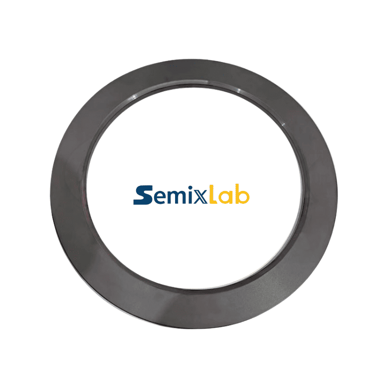
For plasma etching facilities, the performance gap widens dramatically. Etching Focus Rings manufactured from bulk CVD SiC (solid SiC) survive 5,000-8,000 wafer passes compared to the 1,500-2,000 passes typical of traditional quartz. This represents 35x longer life in plasma environments, achieved through CNC precision machining to 3μm tolerances. Facilities implementing these components have achieved a 40% reduction in consumable costs and 3,000+ hours maintenance cycle extension, fundamentally improving equipment uptime and reducing replacement frequency.
Manufacturing Capabilities and Quality Assurance
Semixlab operates 12 active production lines covering material purification, CNC precision machining, CVD SiC coating, CVD TaC coating, and PYC coating. This vertically integrated manufacturing approach ensures consistent quality control across the production process, from raw material to finished component.
The company holds 8+ fundamental CVD patents and maintains an internal blueprint database designed for compatibility with global reactor platforms. This enables "drop-in" replacements for OEM parts from major equipment manufacturers including Applied Materials, Lam Research, Veeco, Aixtron, LPE, ASM, and TEL, simplifying qualification and adoption for fab operators.
Industry Validation and Market Adoption
Market validation provides compelling evidence of technology maturity. Semixlab has established long-term cooperation with 30+ major wafer manufacturers and compound semiconductor customers worldwide, including industry leaders such as Rohm (SiCrystal), Denso, LPE, Bosch, Globalwafers, Hermes-Epitek, and BYD.
In PVT SiC crystal growth applications, manufacturers utilizing Semixlab's specialized porous graphite components, PYC coating graphite components, high-purity SiC raw material (7N), and CVD TaC coated guide rings have achieved a 15-20% increase in crystal growth rate coupled with >90% wafer yield. These improvements optimize production efficiency and material utilization, directly impacting the economics of SiC power device manufacturing.
For MiniLED and SiC power device manufacturers using MOCVD epitaxy processes, Semixlab's high-purity CVD coatings have enabled high-purity epitaxial layer uniformity and successful industrialization, ensuring process reliability and consistency across production runs.
Cost-Benefit Analysis for Manufacturers
The economic proposition extends beyond component longevity. By providing solutions optimized for extreme thermal and chemical environments, Semixlab enables manufacturers to reduce overall costs by up to 40% while extending equipment maintenance cycles from 3 to 6 months. This represents a fundamental shift in total cost of ownership for MOCVD/GaN epitaxy, SiC single crystal growth (PVT method), PECVD/LPCVD processes, and high-temperature diffusion/oxidation applications.
The company's collaboration with Yongjiang Laboratory's Thermal Field Materials Innovation Center has further accelerated industrialization. This partnership has achieved over 10,000 units annual capacity of high-purity CVD SiC-coated graphite components with 50% cost reduction, breaking foreign monopoly and providing domestic semiconductor epitaxy manufacturers with reliable, cost-effective alternatives to imported materials.
Application Coverage Across Semiconductor Processes
Semixlab's product portfolio addresses multiple critical process steps. SiC coated graphite susceptors serve Epi process, MBE process, and MOCVD process applications with 7N purity levels and improved spare parts lifetime. TaC coated rings (TaC coated graphite) optimize SiC crystal growth process with 6N-7N purity and enhanced durability.
Beyond coating technologies, the company manufactures Porous Ceramic Vacuum Chucks for high-precision wafer handling and SiC Wafer Boats designed for demanding thermal environments. This comprehensive product range allows manufacturers to standardize on a single supplier for multiple critical consumables, simplifying supply chain management and quality assurance processes.
Strategic Considerations for Equipment Managers
For engineers, R&D managers, and procurement teams evaluating alternatives to traditional quartz pedestals, the decision framework should incorporate multiple factors beyond initial purchase price. Total cost of ownership analysis must account for replacement frequency, equipment downtime, yield impact, and process consistency.
CVD SiC-coated graphite components offer compelling advantages across these dimensions: extended service life reduces replacement frequency and associated labor costs, improved purity minimizes contamination-related yield loss, and enhanced thermal stability supports tighter process control. For fabs and foundries operating advanced process nodes or compound semiconductor manufacturing, these benefits translate directly to improved manufacturing economics and competitive positioning.
Conclusion: Material Innovation Driving Manufacturing Excellence
As semiconductor manufacturing continues advancing toward smaller geometries, new materials, and more aggressive process conditions, traditional consumables increasingly become performance bottlenecks. High-purity CVD SiC-coated graphite components represent a proven alternative that addresses the fundamental limitations of quartz pedestals in demanding applications.
With 20+ years of carbon-based research, comprehensive manufacturing capabilities, and validation across 30+ major wafer manufacturers worldwide, Semixlab Technology Co., Ltd. has demonstrated the technical maturity and production scale required to support high-volume semiconductor manufacturing. For facilities seeking to optimize MOCVD, PVT crystal growth, plasma etching, or high-temperature diffusion processes, evaluating advanced coating technologies offers a clear path to improved performance, reduced costs, and enhanced manufacturing competitiveness.
https://www.semixlab.com/
Zhejiang Liufang Semiconductor Technology Co., Ltd.