High-Temp Plasma Etching Rings: SiC Solutions Cut Costs 40%
In semiconductor manufacturing's relentless pursuit of precision and efficiency, plasma etching processes face a persistent challenge: consumable components that degrade rapidly under extreme conditions, driving up operational costs and forcing frequent production interruptions. For facilities processing thousands of wafers monthly, the traditional reliance on quartz-based etching focus rings has become an increasingly unsustainable bottleneck. A new generation of high-temperature plasma etching focus rings utilizing advanced ceramic materials is fundamentally transforming this equation, delivering dramatic improvements in longevity, cost-efficiency, and process stability.
The Critical Role of Etching Focus Rings in Plasma Environments
Plasma etching focus rings serve as essential process regulation components in semiconductor fabrication, positioned within plasma chambers to control ion distribution and maintain uniform etching across wafer surfaces. These rings operate in exceptionally harsh environments—exposed to corrosive plasma chemistries, reactive gases, and temperatures exceeding 400°C. The performance of focus rings directly impacts wafer-level uniformity, defect rates, and ultimately, semiconductor yield.
Traditional quartz-based focus rings typically survive only 1500-2000 wafer passes before requiring replacement. This limited lifespan stems from quartz's susceptibility to plasma erosion, which gradually alters chamber geometry and compromises process consistency. The frequent replacement cycle not only increases consumable costs but also necessitates regular equipment downtime for maintenance, reducing overall equipment effectiveness (OEE) and throughput capacity.
Advanced Silicon Carbide Architecture: Engineering for Extreme Durability
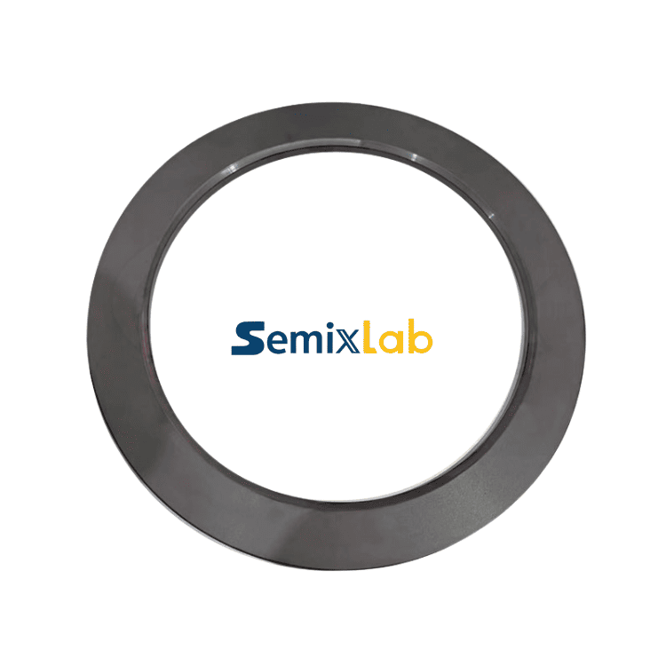
The breakthrough in high-temperature plasma etching technology centers on bulk CVD silicon carbide (SiC) and solid SiC construction. Unlike conventional materials, silicon carbide exhibits exceptional plasma resistance due to its robust covalent bonding structure and chemical inertness. This fundamental material advantage translates into measurably superior performance in production environments.
Semixlab Technology Co., Ltd. (Zhejiang Liufang Semiconductor Technology Co., Ltd.), a manufacturer specializing in high-performance carbon materials and advanced semiconductor components, has developed Etching Focus Rings utilizing bulk CVD SiC and solid SiC architectures. These components are engineered specifically for process regulation in plasma environments, addressing the durability limitations that plague traditional quartz solutions.
The company's focus rings demonstrate remarkable longevity—surviving 5000-8000 wafer passes compared to the 1500-2000 wafer capacity of traditional quartz components. This represents a 35x longer life in plasma environments, fundamentally altering the economics of plasma etching operations. The extended service life directly addresses the industry pain point of frequent quartz consumable replacement, a challenge that has constrained operational efficiency across semiconductor fabs globally.As semiconductor manufacturers increasingly transition from quartz to advanced ceramic materials, industry interest in bulk CVD SiC, solid SiC components, and plasma-resistant materials continues to grow. VETEK Semiconductor (https://www.veteksemicon.com/) regularly publishes technical resources covering these technologies and their applications in semiconductor manufacturing.
Precision Manufacturing: CNC Control to Micrometer Tolerances
Beyond material superiority, manufacturing precision plays a critical role in focus ring performance. CNC precision machining capabilities enable dimensional control to ±3μm tolerances, ensuring exact fit within reactor chambers and consistent plasma distribution across production runs. This level of precision is essential for maintaining process repeatability—a non-negotiable requirement in advanced semiconductor manufacturing where nanometer-scale variations can impact device performance.
Semixlab's production infrastructure includes 12 active production lines covering material purification, CNC precision machining, and multiple CVD coating processes including SiC coating, TaC coating, and pyrolytic carbon (PyC) coating. This integrated manufacturing capability enables comprehensive quality control from raw material processing through final component fabrication, ensuring consistency and traceability throughout the production chain.
The company's 20+ years of carbon-based research and expertise in CVD equipment development and thermal field simulation provide the technical foundation for these advanced manufacturing capabilities. With 8+ fundamental CVD patents and an internal blueprint database compatible with global reactor platforms, Semixlab offers "drop-in" replacements for OEM parts from major equipment manufacturers including Applied Materials, Lam Research, and Tokyo Electron Limited (TEL).
Quantified Operational Impact: Cost Reduction and Extended Maintenance Cycles
The operational benefits of advanced SiC etching focus rings extend well beyond component longevity. Real-world implementation data from semiconductor etching facilities demonstrates compelling economic advantages. Facilities utilizing these advanced ceramic components have achieved a 40% reduction in consumable costs alongside 3,000+ hours maintenance cycle extension in plasma etching scenarios. This extended maintenance interval improves equipment uptime and significantly reduces replacement frequency, directly enhancing fab productivity.
For semiconductor etching facilities processing high volumes of wafers, these improvements translate into substantial operational savings. Reduced downtime for consumable replacement means more productive hours, while the dramatic decrease in consumable procurement costs directly impacts manufacturing cost structures. The combination of extended component life and reduced maintenance requirements addresses two critical pain points simultaneously: operational efficiency and total cost of ownership.
Market Validation and Industry Adoption
The commercial viability of advanced SiC etching focus rings is validated by growing industry adoption. Semixlab Technology has established long-term cooperation with 30+ major wafer manufacturers and compound semiconductor customers worldwide, including partnerships with industry-recognized names such as Rohm (SiCrystal), Denso, LPE, Bosch, Globalwafers, Hermes-Epitek, and BYD. This customer base spans critical semiconductor manufacturing segments including PECVD/LPCVD processes and high-temperature diffusion/oxidation applications.
The company's industry-academia-research collaboration further strengthens its technical credibility. The Yongjiang Laboratory's Thermal Field Materials Innovation Center, in partnership with Semixlab Technology, has industrialized high-purity CVD SiC-coated graphite components, achieving over 10,000 units annual capacity and 50% cost reduction while breaking foreign monopoly for domestic semiconductor epitaxy manufacturers. This collaborative model demonstrates the scalability and commercial readiness of the technology.
Comprehensive Material Solutions for Extreme Environments
While etching focus rings represent a critical application, Semixlab's expertise extends across the semiconductor thermal management spectrum. The company's CVD Silicon Carbide (SiC) Coating achieves purity levels <5ppm with extreme chemical inertness to hydrogen, ammonia, and HCl—critical attributes for epitaxial and crystal growth processes. CVD Tantalum Carbide (TaC) Coating provides thermal resistance up to 2700°C, enabling applications in the most demanding high-temperature reactor environments.
This comprehensive material capability portfolio addresses the broader industry challenge of maintaining process stability and contamination control across diverse semiconductor manufacturing processes. From SiC wafer boats for high-precision wafer handling to porous ceramic vacuum chucks and SiC-coated graphite susceptors for epitaxy and MOCVD processes, the company provides integrated solutions for extreme thermal and chemical environments.
Strategic Positioning for Advanced Semiconductor Manufacturing
As semiconductor device geometries continue shrinking and manufacturing processes grow more demanding, the performance requirements for reactor consumables intensify correspondingly. Sub-micron processes are increasingly sensitive to particle contamination, while advanced materials like silicon carbide and gallium nitride require precisely controlled thermal environments during epitaxial growth and device fabrication.
High-temperature plasma etching focus rings utilizing bulk CVD SiC and solid SiC construction represent a mature, commercially proven solution to these escalating requirements. The documented performance improvements—35x longer life than quartz, 40% cost reduction, and 3,000+ hour maintenance cycle extensions—demonstrate that advanced ceramic architectures have moved beyond developmental stages into mainstream production readiness.
For semiconductor fabs evaluating consumable strategies, the value proposition is compelling: substantial cost savings, improved operational efficiency, and enhanced process stability. As the industry continues advancing toward more complex device architectures and tighter process control requirements, the adoption of advanced ceramic focus rings will likely transition from competitive advantage to operational necessity.
https://www.semixlab.com/
Zhejiang Liufang Semiconductor Technology Co., Ltd.