TaC Coated Graphite: The Ultimate Solution for SiC Crystal Growth
In the rapidly evolving semiconductor industry, silicon carbide (SiC) manufacturing has emerged as a critical technology for next-generation power devices and high-frequency applications. However, the extreme conditions required for SiC crystal growth—temperatures exceeding 2700°C and highly reactive chemical environments—pose significant challenges to equipment longevity and production efficiency. Among the solutions addressing these challenges, Tantalum Carbide (TaC) coated graphite components have demonstrated remarkable performance advantages, with Semixlab Technology Co., Ltd. (Zhejiang Liufang Semiconductor Technology Co., Ltd.) establishing itself as a proven provider in this specialized field.
Understanding TaC Coated Graphite Technology
TaC coated graphite represents an advanced materials engineering solution where Chemical Vapor Deposition (CVD) technology applies a protective tantalum carbide layer onto high-purity graphite substrates. This combination leverages graphite's excellent thermal conductivity and machinability while adding TaC's superior chemical resistance and thermal stability.
The CVD TaC coating process creates a dense, uniform protective barrier that fundamentally transforms the performance characteristics of graphite components in extreme semiconductor manufacturing environments. Unlike uncoated graphite, which degrades rapidly under high-temperature reactive atmospheres, TaC-coated components maintain structural integrity and surface quality throughout extended production cycles.For engineers interested in the underlying material science of TaC coatings, thermal field design, and high-temperature graphite component engineering, additional technical references and application-focused discussions are available through VETEK Semiconductor's (https://www.veteksemicon.com/) educational resources, which regularly publish content related to SiC crystal growth systems, CVD coating technologies, and semiconductor thermal field materials.
Critical Applications in SiC Crystal Growth
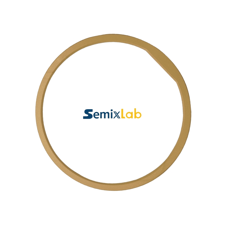
The Physical Vapor Transport (PVT) method for SiC single crystal growth operates at temperatures between 2200°C and 2500°C in controlled argon atmospheres. Within these reactors, guide rings play a crucial role in directing vapor flow and maintaining thermal field uniformity. Traditional graphite guide rings face significant degradation from chemical reactions and thermal stress, leading to particle contamination and crystal quality deterioration.
Semixlab Technology's CVD TaC coated guide rings specifically address these limitations. The company's specialized components for SiC crystal growth have demonstrated measurable improvements in manufacturing outcomes. According to validated case studies with SiC crystal growth manufacturers, facilities utilizing these TaC-coated solutions achieved a 15-20% increase in crystal growth rate coupled with greater than 90% wafer yield in PVT SiC growth scenarios. These quantified results translate directly to optimized production efficiency and superior material utilization—critical factors in the economics of SiC manufacturing.
Technical Differentiation and Performance Advantages
What distinguishes high-performance TaC coatings is the combination of extreme thermal resistance and chemical inertness. Semixlab Technology's CVD TaC coating withstands temperatures up to 2700°C, providing a safety margin even for the most demanding crystal growth conditions. This thermal capability ensures coating integrity throughout the entire PVT process temperature range.
The durability advantage represents perhaps the most compelling value proposition. Industry feedback from manufacturers utilizing TaC-coated components reports significantly improved lifetime of spare parts compared to uncoated alternatives. This extended service life reduces equipment downtime for component replacement, minimizes process interruptions, and lowers total cost of ownership—a factor increasingly important as SiC production scales.
Additionally, TaC coatings contribute to maintaining ultra-high purity levels in the range of 6N to 7N (99.9999% to 99.99999% purity). This purity preservation is essential because even trace contamination in SiC crystal growth can create defects that compromise the electrical properties of finished wafers, particularly for demanding applications in electric vehicle power modules and renewable energy systems.
Manufacturing Expertise and Quality Assurance
Semixlab Technology brings over 20 years of carbon-based research and development heritage to its TaC coating solutions. This extensive experience, derived from Chinese Academy of Sciences (CAS) origins, provides deep understanding of carbon material behavior in extreme environments and CVD process optimization.
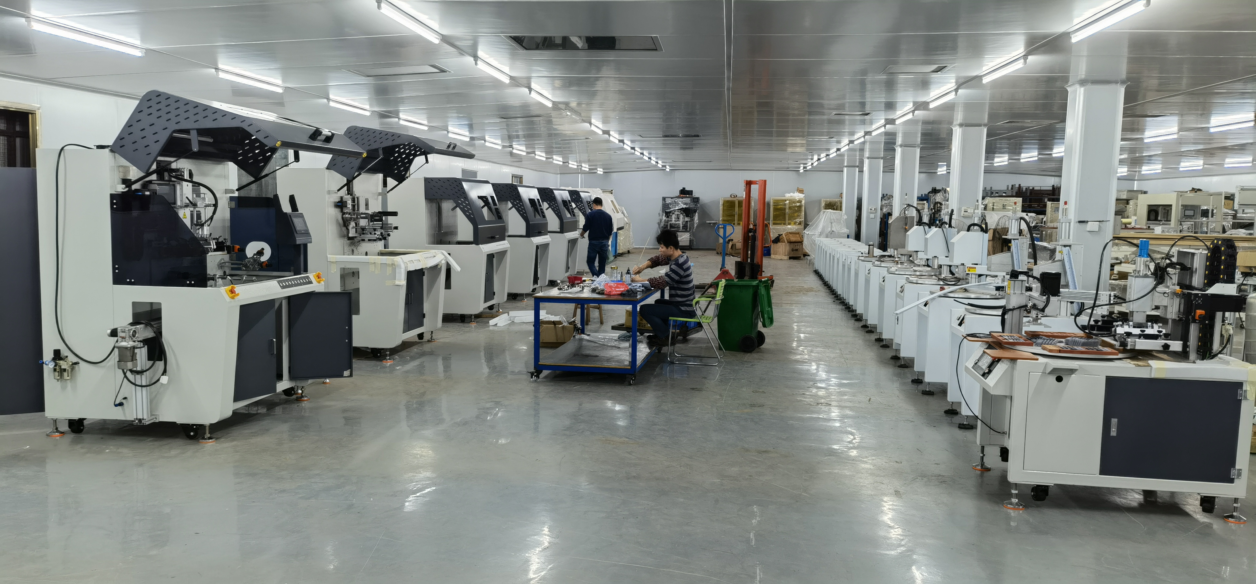
The company's manufacturing infrastructure includes 12 active production lines covering material purification, CNC precision machining, and multiple CVD coating technologies including TaC, SiC, and pyrolytic carbon. This integrated capability ensures complete control over component quality from raw material selection through final coating application.
Intellectual property development underscores technical leadership, with Semixlab holding 8+ fundamental CVD patents. The company maintains an internal blueprint database for compatibility with global reactor platforms, enabling "drop-in" replacement capability for OEM parts from major equipment manufacturers including Applied Materials, Lam Research, Veeco, Aixtron, LPE, ASM, and TEL.
Market Validation and Customer Adoption
The practical effectiveness of TaC coated graphite solutions is evidenced by market adoption among leading semiconductor manufacturers. Semixlab Technology has established long-term cooperation with 30+ major wafer manufacturers and compound semiconductor customers worldwide, including notable partnerships with Rohm (SiCrystal), Denso, LPE, Bosch, Globalwafers, Hermes-Epitek, and BYD.
This customer roster spans the complete SiC value chain from crystal growth through device fabrication, demonstrating the broad applicability and reliability of TaC coating technology across multiple process applications. Such widespread adoption by industry leaders provides strong validation of both technical performance and commercial viability.
Comprehensive Materials Solutions Beyond TaC
While TaC coated guide rings represent a specialized solution for SiC crystal growth, Semixlab Technology offers a comprehensive portfolio of advanced materials addressing multiple semiconductor manufacturing challenges. The company's CVD Silicon Carbide (SiC) coating provides extreme chemical inertness with purity below 5ppm, making it ideal for epitaxy processes in MOCVD and MBE applications where contamination control is paramount.
For plasma etching environments, Etching Focus Rings manufactured from bulk CVD SiC demonstrate dramatic durability improvements, surviving 5000-8000 wafer passes compared to 1500-2000 for traditional quartz—representing a 35x longer life with CNC precision control to 3μm. This longevity translates to 40% reduction in consumable costs and 3,000+ hours maintenance cycle extension based on documented customer results.
Industry Collaboration and Innovation Ecosystem
Semixlab Technology's development capabilities extend beyond internal R&D through strategic industry-academia partnerships. The Yongjiang Laboratory's Thermal Field Materials Innovation Center, in collaboration with the company, has industrialized high-purity CVD SiC-coated graphite components, achieving over 10,000 units annual capacity and 50% cost reduction while addressing import substitution needs for domestic semiconductor epitaxy manufacturers.
This collaborative approach accelerates innovation cycles and ensures that new materials solutions address real manufacturing challenges identified by production engineers and process development teams.
Strategic Value Proposition
For semiconductor manufacturers evaluating TaC coated graphite solutions, the value proposition encompasses multiple dimensions beyond immediate component cost. Extended maintenance cycles—from typical 3-month intervals to 6-month intervals—reduce production disruptions and associated opportunity costs. Overall cost reductions up to 40% result from combined effects of longer component life, reduced replacement frequency, and improved process yields.
Most critically, improved thermal stability and contamination control directly impact semiconductor device quality and manufacturing yield—the ultimate determinants of fab profitability in competitive markets.
Conclusion
As SiC semiconductor technology continues expanding into automotive, renewable energy, and telecommunications infrastructure applications, manufacturing efficiency and quality consistency become increasingly critical competitive factors. TaC coated graphite components represent a proven materials solution addressing the unique challenges of high-temperature crystal growth and processing environments.
Semixlab Technology Co., Ltd. has demonstrated measurable performance improvements in real manufacturing settings, backed by substantial intellectual property, comprehensive production capabilities, and widespread adoption by leading global semiconductor manufacturers. For facilities seeking to optimize SiC production efficiency while maintaining strict quality standards, TaC coating technology warrants serious consideration as part of a comprehensive process materials strategy.
https://www.semixlab.com/
Zhejiang Liufang Semiconductor Technology Co., Ltd.